
Abstract
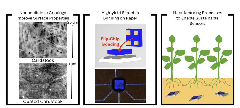
Printed hybrid electronics and sensors achieve increased functionality via the integration of silicon-based chips with printed devices. Paper has gained attention as a substrate for printed devices due to the sustainability and biodegradability of cellulose. Reliable attachment of silicon-based chips onto printed metal traces is essential for manufacturing paper-based printed hybrid sensors. Paper substrates often have high roughness and porosity, leading to infiltration and spreading of screen-printed inks. Here, a nanocellulose coating is used to reduce the roughness of commercial cardstock from 4.23 μm to 0.60 μm, leading to a 1.49 μm reduction in the average trace roughness of screen-printed silver. The improved geometric uniformity results in an 18.1% increase in the yield of flip-chip bonds between test chips and screen-printed silver traces using an anisotropic conductive adhesive. The circuit resistance of prints and the contact resistance of bonds on the coated paper are comparable to those of devices on polyimide, a widely used polymer substrate. In addition, the thermal budget of the nanocellulose coating was investigated by measuring flip-chip bond yield and device resistance as a function of annealing temperature and flip-chip bond parameters.
https://ieeexplore.ieee.org/document/11554473

Figure 1. Test chip and screen-printed pattern used in the experiments. (a) Si test chip with Au traces and bond pads. (b) Screen-printed Ag pattern on a nanocellulose-coated paper substrate. The chips are bonded at the center where the traces converge. (c) Image overlay of screen-printed and Si test chip patterns with labels indicating traces used for the daisy chain (orange) and four-point (red and green) resistance measurements. (d) Flip-chip bonded test chip attached to screen-printed pattern using an anisotropic conductive adhesive.