Abstract

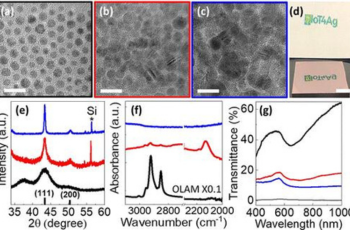
Emerging applications of Internet of Things (IoT) technologies in smart health, home, and city, in agriculture and environmental monitoring, and in transportation and manufacturing require materials and devices with engineered physical properties that can be manufactured by low-cost and scalable methods, support flexible forms, and are biocompatible and biodegradable. Here, we report the fabrication and device integration of low-cost and biocompatible/biodegradable colloidal Cu nanocrystal (NC) films through room temperature, solution-based deposition, and sintering, achieved via chemical exchange of NC surface ligands. Treatment of organic-ligand capped Cu NC films with solutions of shorter, environmentally benign, and noncorrosive inorganic reagents, namely, SCN– and Cl–, effectively removes the organic ligands, drives NC grain growth, and limits film oxidation. We investigate the mechanism of this chemically driven sintering by systemically varying the Cu NC size, ligand reagent, and ligand treatment time and follow the evolution of their structure and electrical and optical properties. Cl–-treated, 4.5 nm diameter Cu NC films yield the lowest DC resistivity, only 3.2 times that of bulk Cu, and metal-like dielectric functions at optical frequencies. We exploit the high conductivity of these chemically sintered Cu NC films and, in combination with photo- and nanoimprint-lithography, pattern multiscale structures to achieve high-Q radio frequency (RF) capacitive sensors and near-infrared (NIR) resonant optical metasurfaces.


