
Abstract
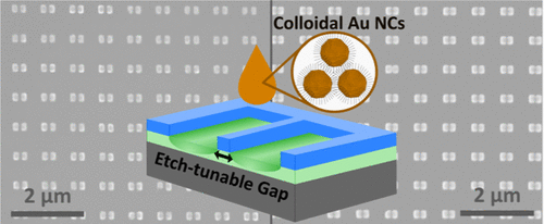
Plasmonic metasurfaces composed of nanodimer repeat units with ultranarrow gaps have strong fields confined to the subwavelength gaps, which can enable resonance wavelength tuning and polarization control. We report a scalable fabrication process that takes advantage of nanoimprint lithography and the solution processability and surface conformability of colloidal nanocrystal dispersions to realize large-area, geometrically engineered nanodimer metasurfaces from a single master template. Geometrical control of the nanodimer gap is achieved through a combination of controlled wet etching of bilayer imprint resists and solution-based nanocrystal deposition and ligand exchange. Using a master template with 50 nm gaps and tailoring the wet etch, nanocrystal concentration, and ligand exchange time, we achieve large-area (1 cm2) metasurfaces with nanogaps tailorable from 72 nm to as narrow as 21 nm, even to the point of fusing the nanorods. We characterize the gap-size-dependent spectral response in the near-infrared, which shows increased electric field confinement and polarization dependence when the gap narrows. This process is promising in its potential for scalable manufacturing and nanogap engineering, using a single master template, of nanodimer metasurfaces, which are of particular interest for applications in refractive index sensing.
https://pubs.acs.org/doi/full/10.1021/acsanm.4c07056
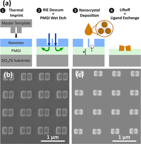
Figure: (a) Schematic overview of the tailorable nanodimer array fabrication process: (1) master template is nanoimprinted into bilayer Nanonex imprint/PMGI undercut resists; (2) dry RIE descum is conducted to expose the PMGI undercut layer and subsequent wet etching is conducted to create nanocavities in the PMGI layer; (3) colloidal Au NC dispersion is deposited onto the patterned samples, conformally filling the nanopatterned cavities, whose geometries differ from the original template and can be described by their radius of curvature r, and the thickness of the remaining PMGI d; and (4) deposited Au NC layer is lifted off and ligand exchange is conducted to induce a dielectric to metallic transition in the deposited Au NC structures. (b) Top-down SEM image of the nanodimer array master template with a 50 nm nanodimer gap used for nanoimprinting. (c) Top-down SEM image of a representative nanodimer array with a narrower 21 nm gap.