
Abstract
Telecommunications and polarimetry both require the active control of the polarization of light. Currently, this is done by combining intrinsically anisotropic materials with tunable isotropic materials into heterostructures using complicated fabrication techniques owing to the lack of scalable materials that possess both properties. Tunable birefringent and dichromic materials are scarce and rarely available in high-quality thin films over wafer scales. Here we report semiconducting, highly aligned, single-walled carbon nanotubes (SWCNTs) over 4″ wafers with normalized birefringence and dichroism values of 0.09 and 0.58, respectively. The real and imaginary parts of the refractive index of these SWCNT films are tuned by up to 5.9% and 14.3% in the infrared at 2,200 nm and 1,660 nm, respectively, using electrostatic doping. Our results suggest that aligned SWCNTs are among the most anisotropic and tunable optical materials known and open new avenues for their application in integrated photonics and telecommunications.
Published in: https://www.nature.com/articles/s41566-024-01504-0#citeas
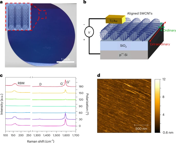
Figure: a, Photograph of a 4 inch wafer with globally aligned, high-purity (99.9999%) semiconducting SWCNTs prepared using a multiple dispersion and sorting process. Inset: the direction of global alignment. b, Diagram of MOSCap geometry that enables the injection of holes and electrons into the SWCNT films by applying negative and positive voltages, respectively. The extraordinary axis (azimuthal direction) and ordinary axis (radial direction) of the SWCNTs are labelled. c, Polarized Raman spectroscopy where the polarization angle is defined relative to the extraordinary axis of the SWCNTs. The RBM, D and G modes are all labelled. The polarization dependence of the intensity of the G+ mode gives an angular variation of 7.2°. d, Atomic force microscopy map of the surface of the SWCNT film showing the high degree of alignment, a thickness of 3.7 nm and a surface roughness of 1.33 nm.